PCBA (Printed Circuit Board Assembly) manufacturing is a crucial process in the production of electronics, encompassing everything from the design of the PCB to the final assembly of components https://arisentecpcb.com/service/pcba/. This article explores the various stages involved in PCBA manufacturing, highlighting the importance of each step in bringing electronic devices to life.
1. Design and Prototyping
PCBA manufacturing begins with the design phase, where engineers create the schematic and layout for the PCB. This involves designing the circuit, determining the placement of components, and ensuring the board meets the electrical and mechanical requirements of the device. CAD software tools like Altium Designer, Eagle, or KiCad are commonly used for this purpose.
Once the design is finalized, a prototype PCB is produced. Prototyping allows engineers to test the functionality of the circuit and make any necessary adjustments before moving to mass production.
2. Component Procurement
After the design is validated, the next step is procuring components. This includes sourcing integrated circuits (ICs), resistors, capacitors, connectors, and other necessary parts. Components are selected based on factors such as cost, availability, and compatibility with the PCB design.
3. PCB Manufacturing
The PCB manufacturing process involves several key steps:
- Substrate Material Selection: Choosing the right substrate material (typically FR4 or similar) based on the application and performance requirements.
- Layer Stackup: Determining the number of layers required and stacking them accordingly.
- Printed Circuit Board Fabrication: This involves creating the actual PCB using a combination of chemical etching, milling, or other manufacturing processes. Advanced PCBs may involve processes like laser drilling for high-density interconnects (HDI).
- Copper Plating: Adding copper layers to the substrate using a process called electroplating.
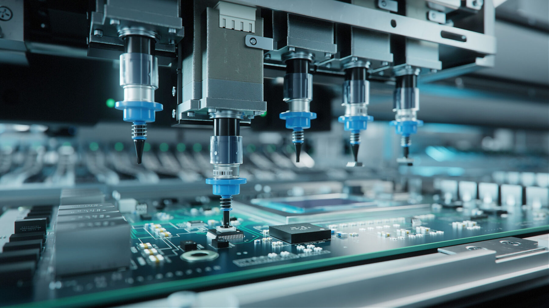
4. Component Placement (SMT Assembly)
Surface Mount Technology (SMT) is the most common method for placing components onto PCBs. This process involves:
- Solder Paste Application: Applying solder paste onto the PCB through a stencil.
- Component Placement: Using pick-and-place machines to accurately position components onto the PCB.
5. Reflow Soldering
Once components are placed, the PCB undergoes reflow soldering. This process involves heating the PCB in a reflow oven to melt the solder paste, creating electrical connections between the components and the PCB.
6. Inspection and Testing
After soldering, the assembled PCB undergoes rigorous inspection and testing. This includes:
- Automated Optical Inspection (AOI): Using cameras to inspect for defects in component placement and solder joints.
- Functional Testing: Verifying the functionality of the PCB and its components.
7. PCBA Packaging
Once the PCB assembly passes inspection and testing, it is ready for packaging. This involves:
- Enclosure Assembly: Integrating the PCB into its final enclosure or housing.
- Final Inspection: A final inspection to ensure all components are correctly assembled and the product meets quality standards.
8. Quality Control and Assurance
Throughout the entire PCBA manufacturing process, quality control and assurance are critical. This involves:
- Process Controls: Monitoring and controlling each step of the manufacturing process to ensure consistency and quality.
- Compliance Testing: Ensuring the PCB assembly meets regulatory and industry standards (e.g., RoHS compliance).
PCBA manufacturing is a complex process that requires precision, expertise, and attention to detail. From initial design to final assembly, each stage plays a crucial role in producing high-quality electronic devices. Advancements in technology continue to drive innovation in PCBA manufacturing, enabling faster production times, higher component densities, and greater reliability in electronic products.